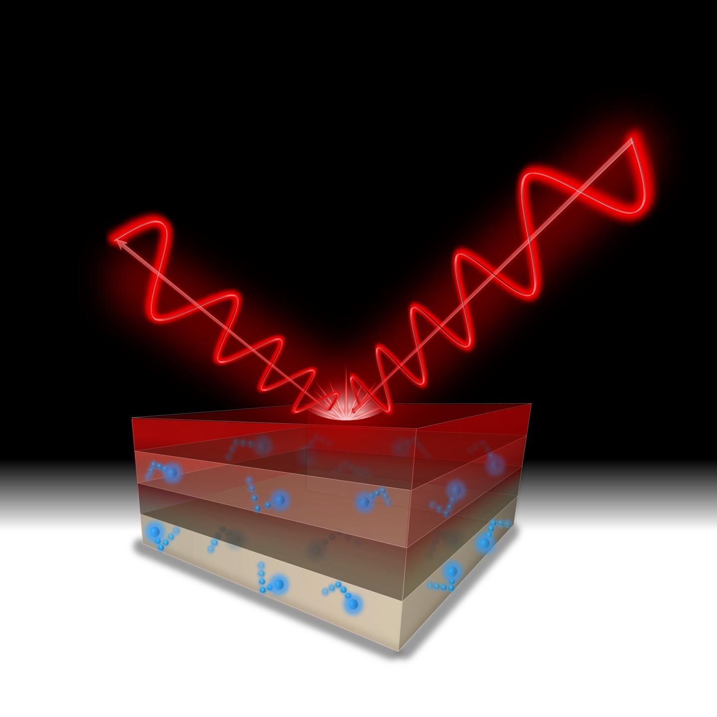

Newly developed ballistic optical materials consist of a composite of two transparent materials, creating a plasmonic material. Credit: Evan Simmons and Kun Li
Electronics are increasingly linked to optical systems, such as when accessing the internet on an electronically operating computer via fiber optic cables.
But meshing optics – which rely on light particles called photons – with electronics – which depend on electrons – are challenging because of their disparate scale. Electrons work on a much smaller scale than light. The mismatch between electronic systems and optical systems means that every time a signal is converted from one signal to another, inefficiency creeps into the system.
Now, a team led by a Purdue University scientist has found a way to create more efficient metamaterials using semiconductors and a new aspect of physics that amplifies the activity of electrons. The study is published in the journal Optics.
This new class of materials has the potential to dramatically increase resolution in medical scans and scientific imaging and dramatically reduce the size of supercomputers, creating a future where scientists can see small things in much more detail and devices are smaller and more powerful.
Scientists have worked for decades to shrink photons down to the nanometer scale to make them more compatible with electrons – a field known as nanophonic. This can be achieved using thin materials and expensive manufacturing techniques to make so-called hyperbolic materials. Using hyperbolic materials, scientists can shrink photons by compressing light, making it easier to communicate with electrical systems.
Evgenii Narimanov, a theoretical physicist and professor of electrical and computer engineering at Purdue, explained, “The most important thing about hyperbolic materials is that they can compress light to almost any scale. If you can make light small, you solve the problem of the breaks between optics and electronics. Then you can make highly efficient opto-electronics. “
The problem lies in making these hyperbolic materials. They usually consist of intertwined layers of metals and dielectrics, and each surface should be as smooth and defect-free as possible at the atomic level, which is difficult, time consuming and expensive.
The solution, Narimanov believes, involves semiconductors. Not, he emphasized, because of something special about the semiconductors themselves. But because scientists and researchers have spent the past 70 years or more working to efficiently produce high-quality semiconductors. Narimanov wondered if he could use and apply that skill to produce new and improved metamaterials.
Unfortunately, semiconductors don’t make inherently good optical metamaterials; they don’t have enough electrons. They can operate at relatively low frequencies, in the mid to far infrared scale. But to improve imaging and detection technologies, scientists need metamaterials that operate in the visible spectrum at the near infrared spectrum, at much shorter wavelengths than the mid and far infrared.
Narimanov and his colleagues discovered and tested an optical phenomenon called ‘ballistic resonance’. In these new optical materials, which combine metamaterial concepts with the atomic precision of monocrystalline semiconductors, free (ballistic) electrons interact with an oscillating optical field.
Synchronizing the optical field with the frequency of movement of the free electrons as they bounce within the boundaries of the thin conductive layers, forming the composite material, causes the electrons to resonate, enhancing the response of each electron and creating a metamaterial is created that works at higher frequencies. Although the researchers couldn’t yet reach the wavelengths of the visible spectrum, they got 60% of the way there.
“We have shown that there is a physical mechanism that makes this possible,” said Narimanov. “Before, people didn’t realize this was something that could be done. We opened the way. We showed that it is theoretically possible, and then we experimentally demonstrated a 60% improvement in operational frequency over existing ones. materials. “
Narimanov came up with the idea and then collaborated with Kun Li, Andrew Briggs, Seth Bank and Daniel Wasserman at the University of Texas, as well as Evan Simmons and Viktor Podolskiy at the University of Massachusetts Lowell. The University of Texas researchers developed the fabrication technology, while the Massachusetts Lowell scientists contributed the full quantum theory and ran the numerical simulations to make sure everything was functioning as planned.
“We will keep pushing this boundary,” Narimanov said. “Even if we are extremely successful, no one will bring semiconductor metamaterials to the visible and near-infrared spectrum in a year or two. It could take about five years. But what we’ve done is provide the materials platform. material where electrons and photons can meet on the same length scale, and we’ve solved it. ”
Broadband enhancement relies on accurate tilt
Kun Li et al, Ballistic Metamaterials, Optics (2020). DOI: 10.1364 / OPTICA.402891
Provided by Purdue University
Quote: Physics Discovery Leads to Ballistic Optical Materials (2020, December 14) Retrieved December 15, 2020 from https://phys.org/news/2020-12-physics-discovery-ballistic-optical-materials.html
This document is protected by copyright. Other than fair treatment for the purposes of private study or research, no part may be reproduced without written permission. The content is provided for informational purposes only.
I was examining some of your blog posts on this site and
I think this site is very instructive! Keep on posting.Leadership