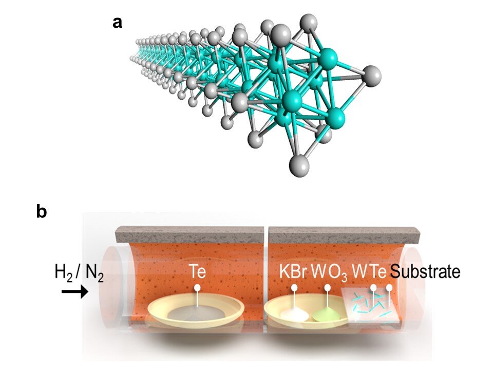
 Illustration of a TMC nanowire (b) Chemical vapor deposition. The ingredients are evaporated in a hydrogen / nitrogen atmosphere and allowed to deposit and self-assemble on a substrate. Reprinted with permission from Ref. 1 Credit: Copyright 2020 American Chemical Society (ACS)")
(a) Illustration of a TMC nanowire (b) Chemical vapor deposition. The ingredients are evaporated in a hydrogen / nitrogen atmosphere and allowed to deposit and self-assemble on a substrate. Reprinted with permission from Ref. 1 Credit: Copyright 2020 American Chemical Society (ACS)
Researchers at Tokyo Metropolitan University have discovered a way to scale self-assembled nanowires of transition metal chalcogenides using chemical vapor deposition. By changing the substrate where the wires form, they can fine-tune how these wires are arranged, from aligned configurations of atomically thin sheets to arbitrary networks of bundles. This paves the way for industrial application in next generation industrial electronics, including energy harvesting and transparent, efficient and even flexible devices.
Electronics is all about making things smaller. For example, smaller functions on a chip mean more computing power in the same space and better efficiency, essential to meet the increasing demands of a modern IT infrastructure powered by machine learning and artificial intelligence. . And as devices get smaller, the same demands are placed on the intricate wiring that connects everything. The ultimate goal would be a wire that is only an atom or two thick. Such nanowires would come to use completely different physics, as the electrons traveling through them increasingly behave as if they were living in a one-dimensional world, not a 3-D world.
In fact, scientists already have materials such as carbon nanotubes and transition metal chalcogenides (TMCs), mixtures of transition metals, and Group 16 elements that can self-assemble into atomic-scale nanowires. The problem is making them long enough and to scale. One way to mass-produce nanowires would be a game changer.
Now a team led by Dr. Hong En Lim and associate professor Yasumitsu Miyata of Tokyo Metropolitan University have come up with a way to make long wires from transition metal telluride nanowires on an unprecedented scale. Using a process called chemical vapor deposition (CVD), they found that they could assemble TMC nanowires in different arrangements depending on the surface or substrate they use as a template. Examples are shown in Figure 2; in (a) nanowires grown on a silicon / silica substrate form a random network of bundles; in (b), the wires assemble in a fixed direction on a sapphire substrate, following the structure of the underlying sapphire crystal. By simply changing where they are grown, the team now has access to centimeter-sized wafers, covered in the desired arrangement, including monolayers, bilayers and bundle networks, all with different uses. They also found that the structure of the wires themselves was highly crystalline and ordered, and that their properties, including their excellent conductivity and 1D-like behavior, matched those in theoretical predictions.
 Scanning electron microscopy image of nanowires grown on a silicon / silica wafer. (b) Atomic force microscopy image of nanowires grown on a crystalline sapphire substrate. (c) Scan transmission electron microscopy image of aligned wires. (d) Transmission electron microscopy image of a single TMC nanowire, viewed from the end, illustrating the structure. Reprinted with permission from Ref. 1 Credit: American Chemical Society (ACS)")
(a) Scanning electron microscopy image of nanowires grown on a silicon / silica wafer. (b) Atomic force microscopy image of nanowires grown on a crystalline sapphire substrate. (c) Scan transmission electron microscopy image of aligned wires. (d) Transmission electron microscopy image of a single TMC nanowire, viewed from the end, illustrating the structure. Reprinted with permission from Ref. 1 Credit: American Chemical Society (ACS)
Having large amounts of long, highly crystalline nanowires will certainly help physicists further characterize and study these exotic structures. Importantly, it is an exciting step to see real-world applications of atomically thin wires, in transparent and flexible electronics, ultra-efficient devices, and energy harvesting applications.
 (a) Illustration of different forms of TMC assembled on the substrates. Cross-sectional transmission electron microscopy images of (b) a nanowire monolayer, (c) a nanowire bilayer, and (d) 3D beam transmission electron microscopy image. Reprinted with permission from Ref. 1 Credit: American Chemical Society (ACS)")
(left) (a) Illustration of different forms of TMC assembled on the substrates. Scanning of transmission electron microscopy images of the cross-section of (b) a nanowire monolayer, (c) a nanowire bilayer, and (d) 3D beam transmission electron microscopy image. Reprinted with permission from Ref. 1 Credit: American Chemical Society (ACS)
From 2-D to 1-D: Atomic quasi ‘1-D’ wires using a carbon nanotube template
Hong En Lim et al, Wafer-scale growth of one-dimensional transition metal telluride nanowires, Nano Letters (2020). DOI: 10.1021 / acs.nanolett.0c03456
Provided by Tokyo Metropolitan University
Quote: Atomic scale nanowires can now be produced to scale (2020, December 24) Retrieved December 24, 2020 from https://phys.org/news/2020-12-atomic-scale-nanowires-scale.html
This document is protected by copyright. Other than fair treatment for the purposes of private study or research, no part may be reproduced without written permission. The content is provided for informational purposes only.