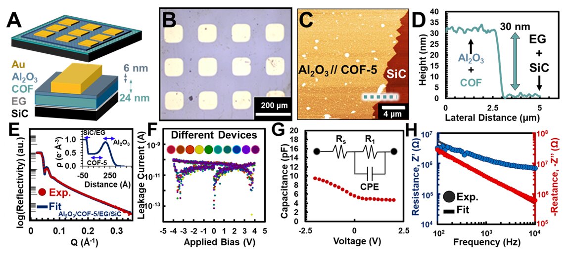

Impedance measurements performed on parallel plate capacitors confirm that COF-5 is a low k dielectric. Credit: Austin Evans
Progress in integrated circuits is measured by adapting, exceeding, or falling short of the speed set forth by Gordon Moore, former CEO and co-founder of Intel, who said the number of electronic components, or transistors, would be per integrated circuit. double every year. That was more than 50 years ago, and surprisingly, his prediction, now called Moore’s Law, came true.
In recent years, the pace was thought to have slowed; One of the biggest challenges in putting more circuits and power on a smaller chip is controlling heat.
A multidisciplinary group featuring Patrick E. Hopkins, a professor in the Department of Mechanical and Aerospace Engineering at the University of Virginia, and Will Dichtel, a professor in Northwestern University’s Department of Chemistry, is inventing a new class of materials with the potential to chips. cool as they keep getting smaller – and to help Moore’s Law stay true. Their work has recently been published in Natural materials
Electrical insulating materials that minimize electrical crosstalk in chips are called “low-k” dielectrics. This material type is the silent hero that enables all electronics by directing the current to eliminate signal erosion and interference; ideally, it can also draw harmful heat from electrical current away from the circuit. The heat problem gets exponential as the chip gets smaller, because not only are there more transistors in a given area, creating more heat in that same area, they are also closer together making it more difficult to dissipate heat.
“Scientists have been looking for a low kk dielectric material that can handle the heat transfer and space issues inherent on a much smaller scale,” Hopkins said. “Although we have come a long way, new breakthroughs will only come when we combine disciplines. For this project we used research and principles from different fields – mechanical engineering, chemistry, materials science, electrical engineering – to solve a very difficult problem. that none of us could solve it alone. “
Hopkins is one of the leaders of UVA Engineering’s Multifunctional Materials Integration initiative, which brings together researchers from multiple engineering disciplines to formulate materials with a wide variety of functionalities.
“Not only was it fascinating to see ‘my’ problem through someone else’s lens in another field, it also sparked ideas that ultimately led to progress. I think we all had that experience,” said Ashutosh Giri, a former UVA Engineering senior scientist and Ph. D. student in Hopkins’ lab, the co-lead author of the Natural materials paper and an assistant professor of mechanical, industrial, and systems engineering at Rhode Island University.
“At the heart of the project was when the chemical team realized the thermal functionality of their material, understood a new dimension of their work, and when the mechanical and materials team understood the level of molecular engineering that is possible with chemistry,” said Giri.
“We take sheets of polymer that are only one atom thick – we call this 2D – and control their properties by laying the sheets in a specific architecture,” said Dichtel.
“Our efforts to improve methods to produce high quality 2-D polymer films have made this partnership possible.”
The team is applying this new class of material to try to meet the requirements of miniaturizing transistors on a dense chip, Dichtel said.
“This has enormous potential for use in the semiconductor industry, the chip manufacturing industry. The material has both a low electrical conductivity, or ‘low-k’, and high heat transfer,” he said.
This combination of features was recently identified by the International Roadmap for Semiconductors as a prerequisite for next-generation integrated circuits.
“For this project, we’re focusing on the thermal properties of this new material class, which is fantastic, but even more exciting is that we’re just scratching the surface,” said Austin Evans, a Ph.D. student in Dichtel’s lab in Northwestern and first co-author on the Natural materials paper. “Developing new classes of materials with unique combinations of properties has an astonishing technological potential.
“We are already researching this new class of materials for many applications, such as chemical detection. We can use these materials to determine – ‘meaning’ – which chemicals and how many of those chemicals are in the air. This has far-reaching consequences. For example, knowing about the chemicals in the air can optimize food storage, transportation and distribution to reduce global food waste. As we continue to explore, we will likely discover even more properties unique to these new materials , ”Evans said.
Can a new 2D material ensure that semiconductors become smaller, stronger, better and faster?
Austin M. Evans et al, Heat-conducting ultra-low-k dielectric layers based on two-dimensional covalent organic frameworks, Natural materials (2021). DOI: 10.1038 / s41563-021-00934-3
Provided by University of Virginia
Quote: To help researchers keep pace with Moore’s Law by exploring a new material class (2021, March 18), retrieved March 18, 2021 from https://phys.org/news/2021-03-pace-law-exploring -material-class.html
This document is copyrighted. Other than fair treatment for the purposes of private study or research, no part may be reproduced without written permission. The content is provided for informational purposes only.